SINGLE PIN NET REPORT
Introduction
With complex, multi-sheet schematics and large components which may span several elements and include multiple NC pins it's not at all easy to verify that each connection has been considered and correctly handled. It's surprisingly easy to miss a connection on the schematic and not realise until much later in the layout (if at all!). Worse still, since the connection is missing from the schematic there will be no ratsnest lines on the layout and the connectivity report will have no knowledge of the problem.
The single pin net report in Project Notes is designed to help customers who want an auditable way to ensure that each connection or NC pin has received designer attention.
Generating the Report
To generate the single pin report:
- Open project notes and select the single pin report
from the available templates. If Project Notes is open (and unlocked!)
select new project note from the File
menu and then the single pin report from the available templates.
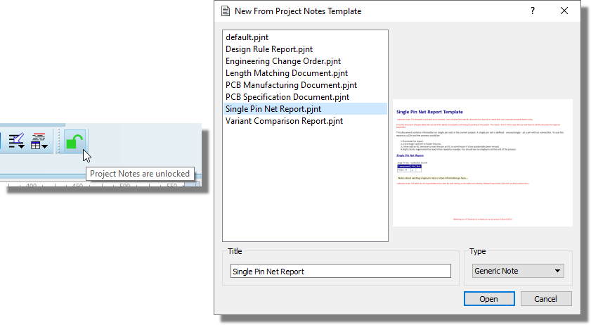
- The report will be automatically generated with the data table listing all component pins which are not connected to anything but which also are not explicitly marked as NC pins.
The table has three columns, Component, Pin and Net, and it closes with a Total row. The total carries a tick when the count is zero and a cross when it is not, which is what makes the report an auditable artefact: a ticked total is the evidence that every pin on the design has been accounted for.
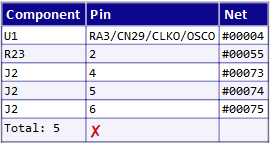
The goal of the report is that either there are no entries in the table (all pins are accounted for) or that each entry in the report is explained textually underneath so that a recorded decision has been made for each case.
The Workflow
- Generate the report as above.
- Find the pins in the report via design explorer.
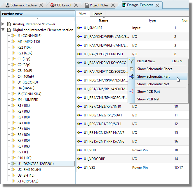
- Attach an NC terminal to the pin to explicitly mark it as NC, or wire
it if it is mistakenly NC.
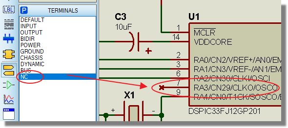
- Rinse and repeat for other NC pins.
Dragging project notes module into separate space (split screen) is helpful here if you have multiple monitors.
You can also mark pins as NC in the packaging tool but this of course is then not visible in a schematic printout.
It's assumed of course that over time users needing to work with this level of verification will actually place NC terminals against NC pins at design time and so very little if any work will be required at this verification phase.